6
RF Device Data
Freescale Semiconductor
MRF6S21050LR3 MRF6S21050LSR3
TYPICAL CHARACTERISTICS
100
13
16.5
3
8
64
Pout, OUTPUT POWER (WATTS) CW
10
16
15
14
56
48
40
32
η
D
, DRAIN EFFICIENCY (%)
G
ps
, POWER GAIN (dB)
15.5
14.5
13.5
VDD
= 28 Vdc
IDQ
= 450 mA
f = 2140 MHz
ηD
Gps
IM3 (dBc), ACPR (dBc)
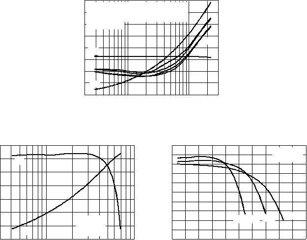
Figure 7. Intermodulation Distortion Products
versus Tone Spacing
1 10010
?60
?10
0.01
7th Order
TWO?TONE SPACING (MHz)
VDD
= 28 Vdc, P
out
= 60 W (PEP), I
DQ
= 450 mA
Two?Tone Measurements
(f1 + f2)/2 = Center Frequency of 2140 MHz
5th Order
3rd Order
?20
?30
?40
?50
Figure 8. Pulsed CW Output Power versus
Input Power
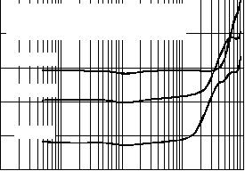
Figure 9. 2-Carrier W-CDMA ACPR, IM3, Power Gain
and Drain Efficiency versus Output Power
0
?60
Pout, OUTPUT POWER (WATTS) AVG. W?CDMA
40
?20
25
?30
20
?35
15
?40
5
?50
0.2 10 301
?45
10
36
52
P3dB = 48.66 dBm (73.43 W)
Pin, INPUT POWER (dBm)
VDD
= 28 Vdc, I
DQ
= 450 mA
Pulsed CW, 8 μsec(on), 1 msec(off)
f = 2140 MHz
50
48
46
44
29 3230
31 3533 34
Actual
Ideal
P1dB = 47.89 dBm (61.52 W)
51
49
45
47
28
Figure 10. Power Gain and Drain Efficiency
versus CW Output Power
Figure 11. Power Gain versus Output Power
Pout, OUTPUT POWER (WATTS) CW
IM3
Gps
η
D
, DRAIN EFFICIENCY (%), G
ps
, POWER GAIN (dB)
IMD, INTERMODULATION DISTORTION (dBc)
P
out
, OUTPUT POWER (dBm)
G
ps
, POWER GAIN (dB)
VDD
= 24 V
09010
20 30
40 50 60 70 80
100
12
17
14
13
15
14.5
16
IDQ
= 450 mA
f = 2140 MHz
30
?55
ηD
ACPR
28
V
32
V
0.1
35
?25
16.5
15.5
13.5
12.5
VDD= 28 Vdc, IDQ
= 450 mA, f1 = 2135 MHz
f2 = 2145 MHz, 2 x W?CDMA, 10 MHz @ 3.84 MHz
Channel Bandwidth, PAR = 8.5 dB @ 0.01%
Probability (CCDF)
16
24


发布紧急采购,3分钟左右您将得到回复。
相关PDF资料
MRF6S21060NR1
MOSFET RF N-CH 28V 14W TO270-4
MRF6S21100HSR5
MOSFET RF N-CHAN 28V 23W NI-780S
MRF6S21100NR1
MOSFET RF N-CH 28V 23W TO270-4
MRF6S21140HSR5
MOSFET RF N-CHAN 28V 30W NI-880S
MRF6S21190HSR5
MOSFET RF N-CH 54W NI880S
MRF6S23100HSR5
MOSFET RF N-CHAN 28V 20W NI-780S
MRF6S23140HSR5
MOSFET RF N-CHAN 28W 28W NI-880S
MRF6S24140HS
IC MOSFET RF N-CHAN NI-880S
相关代理商/技术参数
MRF6S21060BR1
制造商:Freescale Semiconductor 功能描述:
MRF6S21060MBR1
功能描述:MOSFET RF N-CH 28V 14W TO272-4 RoHS:否 类别:分离式半导体产品 >> RF FET 系列:- 产品目录绘图:MOSFET SOT-23-3 Pkg 标准包装:3,000 系列:- 晶体管类型:N 通道 JFET 频率:- 增益:- 电压 - 测试:- 额定电流:30mA 噪音数据:- 电流 - 测试:- 功率 - 输出:- 电压 - 额定:25V 封装/外壳:TO-236-3,SC-59,SOT-23-3 供应商设备封装:SOT-23-3(TO-236) 包装:带卷 (TR) 产品目录页面:1558 (CN2011-ZH PDF) 其它名称:MMBFJ309LT1GOSMMBFJ309LT1GOS-NDMMBFJ309LT1GOSTR
MRF6S21060MR1
功能描述:MOSFET RF N-CH 28V 14W TO270-4 RoHS:否 类别:分离式半导体产品 >> RF FET 系列:- 产品目录绘图:MOSFET SOT-23-3 Pkg 标准包装:3,000 系列:- 晶体管类型:N 通道 JFET 频率:- 增益:- 电压 - 测试:- 额定电流:30mA 噪音数据:- 电流 - 测试:- 功率 - 输出:- 电压 - 额定:25V 封装/外壳:TO-236-3,SC-59,SOT-23-3 供应商设备封装:SOT-23-3(TO-236) 包装:带卷 (TR) 产品目录页面:1558 (CN2011-ZH PDF) 其它名称:MMBFJ309LT1GOSMMBFJ309LT1GOS-NDMMBFJ309LT1GOSTR
MRF6S21060N
制造商:FREESCALE-SEMI 功能描述:
MRF6S21060NBR1
功能描述:射频MOSFET电源晶体管 2170MHZ 14W RoHS:否 制造商:Freescale Semiconductor 配置:Single 晶体管极性: 频率:1800 MHz to 2000 MHz 增益:27 dB 输出功率:100 W 汲极/源极击穿电压: 漏极连续电流: 闸/源击穿电压: 最大工作温度: 封装 / 箱体:NI-780-4 封装:Tray
MRF6S21060NR1
功能描述:射频MOSFET电源晶体管 2170MHZ 14W RoHS:否 制造商:Freescale Semiconductor 配置:Single 晶体管极性: 频率:1800 MHz to 2000 MHz 增益:27 dB 输出功率:100 W 汲极/源极击穿电压: 漏极连续电流: 闸/源击穿电压: 最大工作温度: 封装 / 箱体:NI-780-4 封装:Tray
MRF6S21060NR1_08
制造商:FREESCALE 制造商全称:Freescale Semiconductor, Inc 功能描述:RF Power Field Effect Transistors N-Channel Enhancement-Mode Lateral MOSFETs
MRF6S21100HR3
功能描述:射频MOSFET电源晶体管 HV6 23W W-CDMA RoHS:否 制造商:Freescale Semiconductor 配置:Single 晶体管极性: 频率:1800 MHz to 2000 MHz 增益:27 dB 输出功率:100 W 汲极/源极击穿电压: 漏极连续电流: 闸/源击穿电压: 最大工作温度: 封装 / 箱体:NI-780-4 封装:Tray
